
Electronic components have long been connected to electrical circuits via two electrical terminals, limiting the performance and functionality of systems. However, researchers at the University of Science and Technology of China (USTC) have made significant strides in developing a new three-terminal diode that can both emit and detect light. This breakthrough, detailed in a recent paper published in Nature Electronics, holds great promise for the advancement of wireless communication and light-driven computing systems.
Lead author for the paper, Prof. Haiding Sun, explained that the inspiration behind the development of the three-terminal diode stemmed from the inherent limitations of traditional two-terminal devices, such as the p-n diode. By enhancing the functionality and performance of conventional optoelectronic devices, Sun and his team have paved the way for the implementation of optical wireless communication (OWC) and optoelectronic logic gates (OELGs) for cutting-edge optically controlled computing technologies.
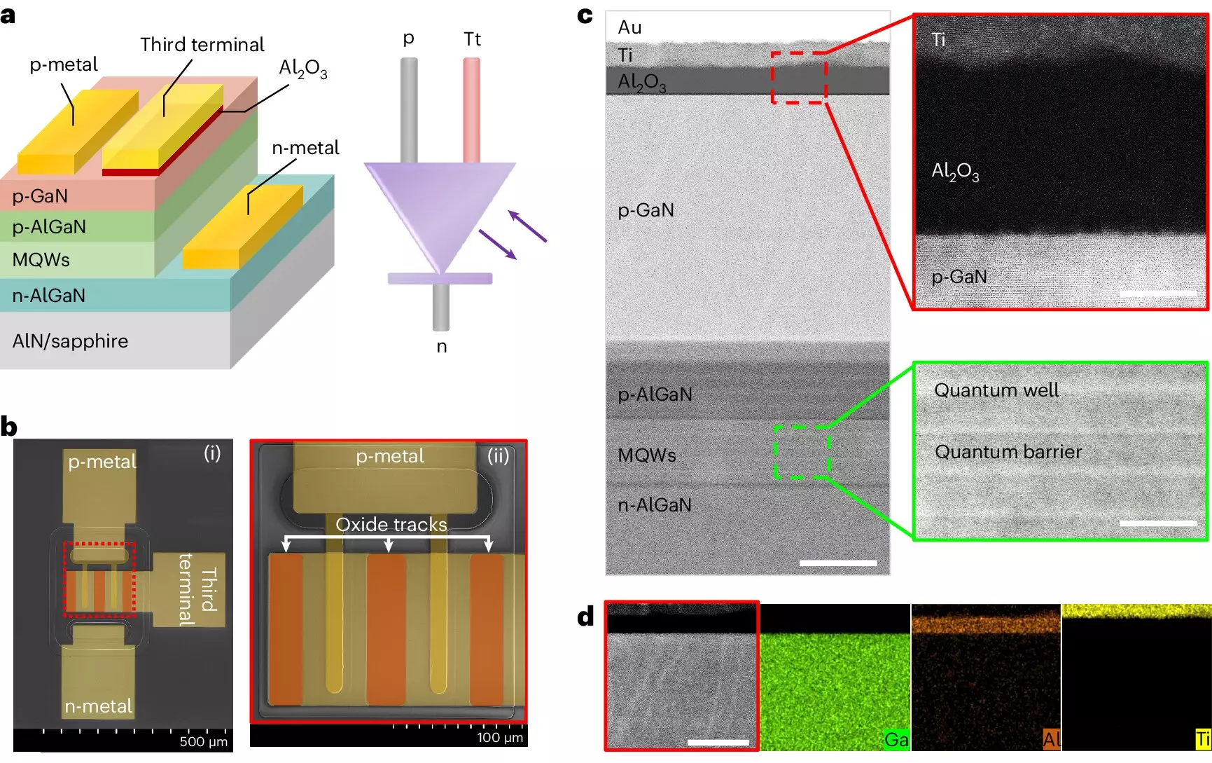
A New Approach to Optoelectronic Devices
The three-terminal diode designed by the USTC research team combines a traditional gallium nitride-based p-n diode with a newly introduced third terminal consisting of a metal/Al2O3 dielectric layer directly applied to the p-GaN layer. This innovative design allows the device to modulate light intensity by adjusting the bias applied to the third terminal, significantly increasing the modulation bandwidth when operating as a light emitter. Furthermore, as a photodetector, the device leverages voltage and incident light inputs to establish reconfigurable NAND and NOR optoelectronic logic gates, showcasing its versatility.
It is important to note that the new three-terminal diode has shown significant improvements in enhancing the modulation bandwidth, exceeding current OWC systems that rely on classic light-emitting p-n diodes. This advancement not only enhances data transmission speeds but also provides a more reliable and efficient method for transmitting information.
Future Implications and Development
As the research team continues to refine the performance of the three-terminal diode, there is a growing potential for integration with other optoelectronic materials and systems. Sun emphasized the importance of exploring techniques to further enhance the capabilities of the diode, paving the way for the development of multifunctional and integrated electronic and optoelectronic systems.
Moving forward, the innovative approach taken by the USTC research team not only holds promise for Gallium Nitride (GaN) materials but also opens up possibilities for other semiconductor platforms. This breakthrough in three-terminal diode technology could revolutionize OWC systems, enabling faster data transmission speeds and the development of advanced optically driven computing systems.
The development of the new three-terminal diode marks a significant breakthrough in the field of optoelectronics. By pushing the boundaries of traditional two-terminal devices, the USTC research team has unlocked new possibilities for highly performing wireless communication and light-driven computing systems. This innovative approach sets the stage for future advancements in integrated photonics and the development of cutting-edge optoelectronic technologies.
Leave a Reply
You must be logged in to post a comment.