
Semiconductors serve as the backbone of modern technology, powering everything from smartphones to solar cells. Their effectiveness hinges not just on the materials themselves but on the behavior of electron charges within these materials. Recent groundbreaking advancements made by researchers from UC Santa Barbara have offered an unprecedented glimpse into how electric charges traverse the interface of two distinct semiconductor materials. By employing innovative scanning ultrafast electron microscopy techniques, the team has visualized the movement of these charges for the first time, sparking new possibilities for semiconductor research and applications.
Exploring the Heart of Photocarrier Dynamics
At the center of this study is the phenomenon of photocarriers—the energized electrons that move through semiconductor materials when exposed to light. When sunlight strikes materials such as silicon or germanium, it excites electrons, allowing them to drift away from their paired “holes.” This activity generates an electric current, which is essential for the operational efficacy of devices such as solar panels. However, a critical challenge lies in the brief lifespan of these photocarriers; they typically lose much of their energy within picoseconds, a minuscule fragment of time in the grand tapestry of physics. As a result, the harvestable energy remains inefficient compared to their initial energetic state.
Understanding the dynamics of these energetic electrons not only enhances knowledge about energy production but also helps in addressing potential pitfalls, such as excess heat generation, which can detrimentally affect semiconductor performance. Consequently, exploring and visualizing how these hot carriers behave as they transition between different materials is pivotal for researchers and engineers alike.
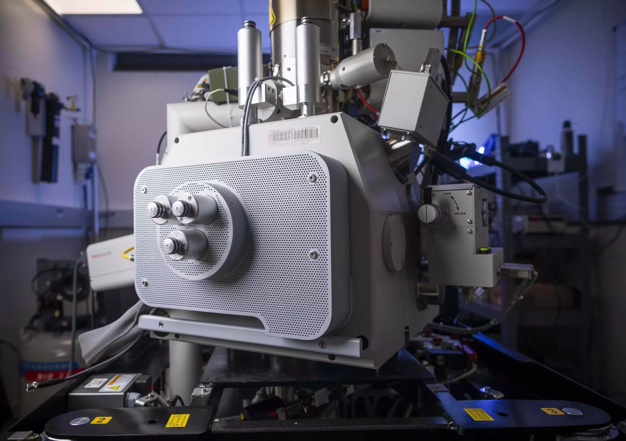
The advent of the scanning ultrafast electron microscopy (SUEM) method has revolutionized the way researchers observe the behaviors of electrons in semiconductor materials. Led by Associate Professor Bolin Liao, this study leverages SUEM’s capabilities to focus on a silicon-germanium heterojunction—a combination of two widely utilized semiconductor materials. The research achieved results that seemed ambitious, if not impossible, just a decade ago.
The technique utilizes ultrafast laser pulses as an effective shutter to visualize the fleeting moments in which electrons move through semiconductor interfaces. As the electron beam scans the material surface, it is synchronized with optical pump beams that excite the electrons. The precision of this imaging allows scientists to observe the unique attributes of hot carrier dynamics within milliseconds of time, showcasing how the charges evolve as they migrate across the heterojunction.
The observations yielded absorbing insights into charge behaviors, particularly focusing on the distinctions in electron movement across materials. When electrons are excited in the uniform sections of silicon or germanium, they exhibit high velocities due to their elevated energy levels. Conversely, those excited near the junction experience a noticeable slowdown because some of these charges are trapped by the potential barrier at the junction. This trapping phenomenon reduces carrier mobility, posing significant implications for the performance of semiconductor devices designed to effectively collect and separate these hot carriers.
Understanding these trapping effects is not merely an academic exercise; it has profound implications for semiconductor design and functionality. While the theoretical basis for these behaviors already existed, the ability to capture and visualize them experimentally provides a new dimension to this field of inquiry—a dimension that could influence future semiconductor development strategies.
A Legacy of Semiconductor Innovation
This research is, in many ways, a culmination of several decades of semiconductor innovation. The concept of heterojunctions was first introduced by former UCSB Professor Herb Kroemer back in 1957, when he rightly asserted that “the interface is the device.” Kroemer’s foresight laid the groundwork for what would become foundational principles in microchip technology. The recent breakthroughs at UCSB reaffirm the ongoing relevance of his vision, highlighting how utilizing advanced techniques can breathe new life into established theories and lend empirical support to long-held beliefs.
In studying these intricate dynamics at the semiconductor interface, we are not merely cataloging electrons; we are unlocking the potential for groundbreaking advancements in energy efficiency, electronic devices, and telecommunications. This research illuminates not just the potential of semiconductor materials but also the path forward for innovative technology that may one day revolutionize our relationship with energy and information.
The capability to visualize hot photocarrier activity at heterojunctions signifies a new chapter in semiconductor research—a chapter that promises to deepen our understanding of materials and the phenomena that govern their functionality in the increasingly electric future.
Leave a Reply
You must be logged in to post a comment.