
Recent advancements in quantum sensing technology have led to the development of a new 2D quantum sensing chip using hexagonal boron nitride (hBN). This innovative chip has the capability to detect temperature anomalies and magnetic fields in any direction, marking a significant breakthrough in the field of quantum technology. The sensor is remarkably thinner compared to existing quantum sensors, offering a more cost-effective and versatile solution for magnetometry.
Traditionally, quantum sensing chips have been fabricated using diamond due to its robust nature. However, diamond-based sensors are limited in their ability to detect magnetic fields only when aligned in a specific direction. This alignment constraint results in large blind spots, necessitating the use of multiple sensors at varying degrees of alignment for accurate measurements. Moreover, the rigid and three-dimensional structure of diamond sensors restricts their ability to closely interact with non-smooth samples.
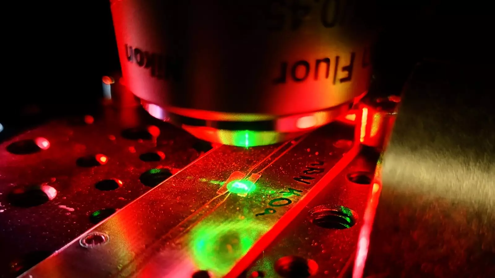
Researchers at TMOS and RMIT University, led by Jean-Philippe Tetienne and Igor Aharonovich, are at the forefront of developing a new quantum sensing platform utilizing hBN. Unlike diamond, hBN crystals consist of atomically thin sheets that are flexible, allowing the sensing chips to conform to the shape of the sample under study. This flexibility enables the sensors to get much closer to the sample, enhancing the accuracy and efficiency of measurements.
Identification of Novel Carbon-Based Defect
A carbon-based defect with an unidentified atomic structure was discovered in hBN, exhibiting the unique ability to detect magnetic fields in any direction. Through a Rabi measurement experiment, researchers determined that this defect behaves as a spin half system, enabling the sensor to detect magnetic fields with high precision. By leveraging electrical excitation, the carbon defect can be controlled similar to the boron vacancy defect in hBN, opening up new possibilities for quantum sensing applications.
The research team successfully demonstrated a hBN sensing chip that utilizes both the carbon-based spin defect and the boron vacancy defect simultaneously to measure magnetic field and temperature. This groundbreaking achievement represents the first magnetic imaging conducted using the unidentified carbon defect, showcasing the potential of hBN as a versatile material for quantum sensing applications.
The unique properties of hBN, including its 2D form factor and isotropic sensing capabilities, hold immense promise for a wide range of applications. From in-field identification of magnetic geological features to radio spectroscopy across a broader band, hBN quantum sensors offer unprecedented opportunities for exploring new physics and advancing quantum technology. With the ongoing research focused on identifying atomic defects in hBN, the potential for engineering optimized sensor devices is within reach.
Overall, the development of quantum sensing technology using hBN represents a significant leap forward in the field of quantum materials and sensor systems. The innovative capabilities of hBN, combined with the expertise of researchers in leveraging its properties, are paving the way for transformative applications in quantum sensing and beyond.
Leave a Reply
You must be logged in to post a comment.