
As electronics continue to advance, researchers are constantly searching for new materials to enhance the performance of electronic devices beyond the limitations of silicon-based transistors. One of the most promising candidates in this quest is two-dimensional (2D) semiconductors. These materials offer unique properties that could significantly improve the electrostatic control and ON-state performances of short-channel field-effect transistors (FETs). With their atomically thin structure and high carrier mobilities, 2D semiconductors hold great potential for revolutionizing the electronics industry.
However, despite their numerous advantages, 2D semiconductors are not without their challenges. One significant limitation is the high contact resistances associated with Fermi-level pinning effects, which can hinder their performance in transistors. Addressing this issue is crucial for the successful integration of 2D semiconductors in electronic devices on a large scale. Recently, researchers at Peking University and Chinese Academy of Sciences introduced a novel yttrium-doping strategy to overcome this key limitation, opening up new possibilities for the effective use of 2D semiconductors in electronics.
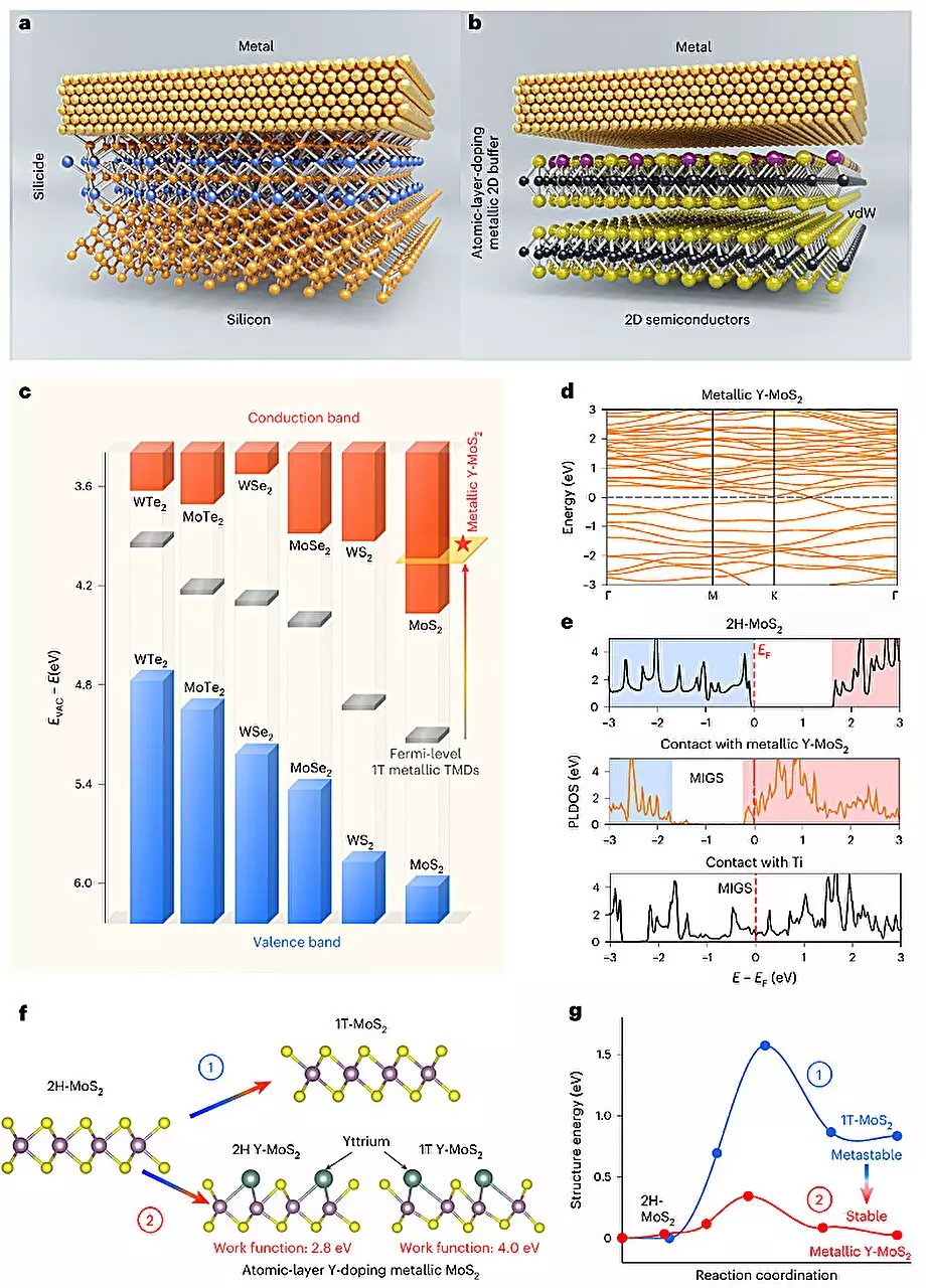
The groundbreaking strategy developed by the researchers involves converting semiconducting molybdenum disulfide (MoS2) into metallic MoS2 through yttrium doping. By adding a semi-metal layer between a metal electrode and the 2D semiconductor, the researchers were able to enhance the efficiency of carrier injection, improving band alignment and facilitating the fabrication of ohmic contacts for 2D transistors. This innovative approach draws inspiration from the traditional silicide structure used in silicon-based transistors, offering a new perspective on addressing the challenges of 2D electronics.
Plasma-Deposition-Annealing Method
Central to the researchers’ approach is the plasma-deposition-annealing (PDA) method, which enables yttrium doping in the surface layer of MoS2. By treating patterned local contact areas with low-power soft plasma to generate active sites, the researchers were able to deposit a Y/Ti/Au stacked metal, with a 1 nm-thick active metal Y serving as a solid-state doping source. The Y atoms diffuse into the active sites through plasma treatment, and they are then activated in the top layer of the material through high-temperature annealing in an inert gas environment. This PDA doping process demonstrates great thermal stability post-annealing and is compatible with advanced-node wafer-scale integration, highlighting its potential for practical application in electronics.
Rare Earth Element Yttrium Doping-Induced 2D Phase Transition
The researchers also introduced a new concept in their study, known as “rare earth element yttrium doping-induced 2D phase transition.” This phase transition represents the metallization observed in MoS2 following the application of the yttrium doping strategy. The development of a selective-area single-atomic-layer surface doping technique marks a significant breakthrough, pushing the doping depth to the atomic layer limit of 0.5 nanometers. This achievement overcomes traditional engineering limitations and sets the stage for the development of ultra-short MoS2-based channel ballistic transistors with superior performance.
Future Implications
Looking ahead, the researchers are optimistic about the potential of their yttrium-doping strategy in advancing 2D electronics. The ultra-short MoS2-based transistors developed through this approach have demonstrated excellent performance as ohmic contacts and possess impressive switching capabilities. These findings pave the way for the development of new sub-1 nanometer node chips that could deliver remarkable performance while consuming less power than conventional chips. The researchers now aim to further enhance their approach by developing equally impressive p-type ohmic contacts suitable for 2D semiconductors, ushering in a new era of electronics innovation.
Leave a Reply
You must be logged in to post a comment.