
The rapid advancement of artificial intelligence (AI) and its increasing reliance on massive data processing capabilities have amplified the demand for advanced memory solutions. Conventional data storage technologies, particularly flash memory, face challenges in keeping up with these demands. Therefore, the need for innovative memory systems that can provide high bandwidth and efficiency is critical for the next generation of computationally intensive applications. Recent breakthroughs in the field of ultrafast flash memory using two-dimensional (2D) materials offer a promising pathway to achieve these goals.
Flash memory, as a non-volatile storage medium, has dominated the market due to its ability to retain data even without power. However, existing flash memory technologies often struggle with speed and efficiency, particularly in the context of AI applications requiring rapid data access and processing capabilities. The slow transfer rates of traditional flash memories may hinder the overall performance of data-intensive AI workloads, leading to the exploration of alternatives that can provide superior performance.
The limitations of current flash memory technologies present significant hurdles; thus, researchers are now focused on the potential of ultrafast flash memory, particularly those leveraging novel materials that can significantly enhance speed and efficiency. Among these, 2D materials such as molybdenum disulfide are emerging as front-runners due to their unique electronic properties, which may allow for much faster data processing capabilities compared to traditional materials.
A breakthrough achieved by researchers at Fudan University represents a significant step towards the practical application of ultrafast flash memory. In a study published in *Nature Electronics*, the team developed a new integration method that successfully combined multiple ultrafast 2D flash memory devices into a cohesive array. They achieved an impressive yield of over 98% while integrating as many as 1,024 devices, a milestone that indicates the potential for large-scale commercialization.
The integration technique employed various advanced processes, including lithography and thermal atomic layer deposition. By utilizing these sophisticated fabrication methods, the researchers were able to create memory devices with distinct tunneling barrier configurations, enhancing their performance metrics. This multifaceted approach signifies that it is possible to fabricate ultrafast flash memory devices not only efficiently but also reliably.
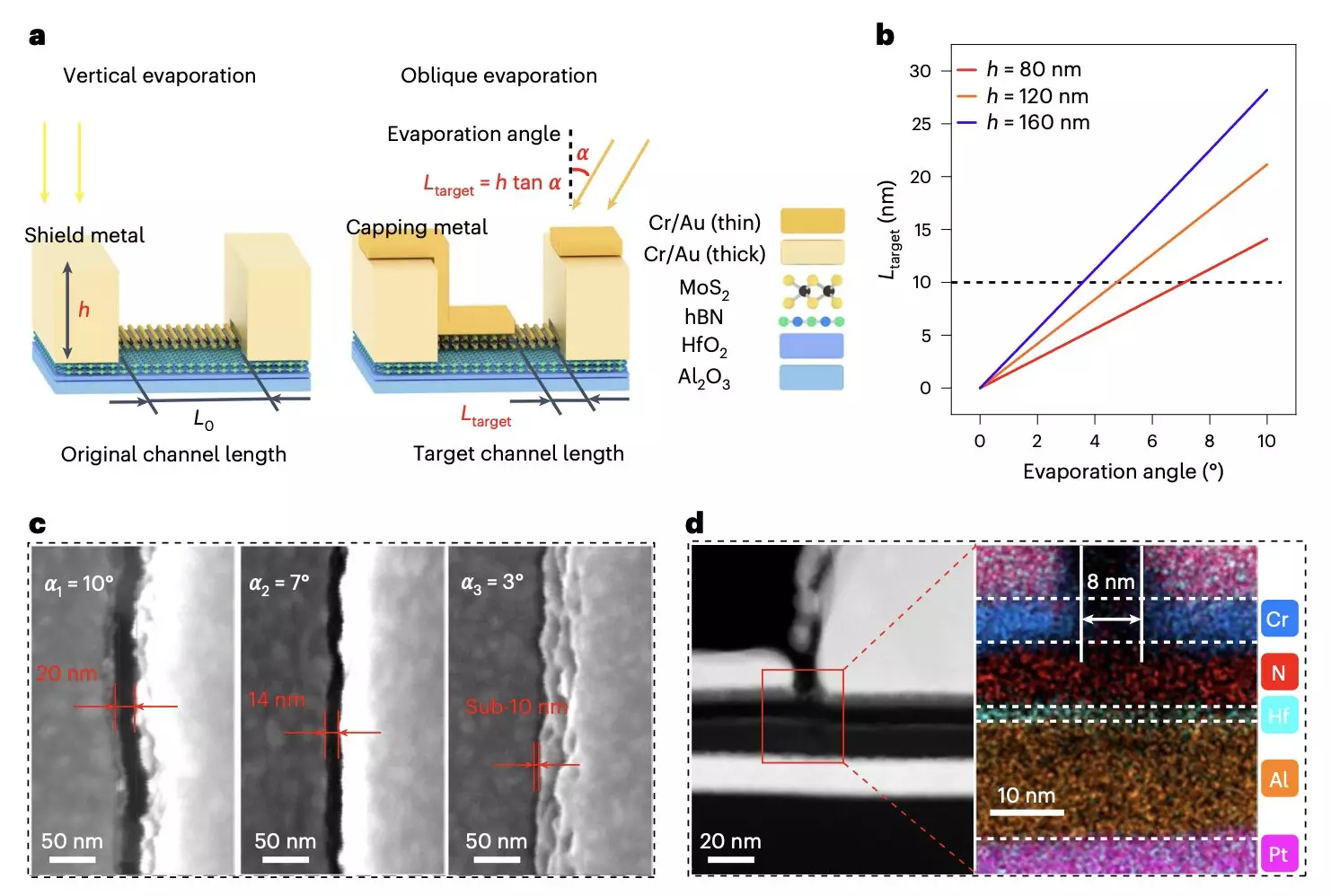
What makes this advancement particularly remarkable is the team’s ability to reduce the channel lengths of these flash memory devices to sub-10 nm, a feat that is below the traditional physical limits associated with silicon-based flash memory. The results of the experiments showcased that these ultrafast devices not only retained non-volatile capabilities but could also store up to four bits of information—indicating an increase in data density alongside improved processing speeds.
The researchers demonstrated that their ultrafast flash memory could maintain robust endurance, further solidifying its suitability for diverse applications, including those in AI and machine learning, where high performance and reliability are paramount. This confluence of high yield, speed, and endurance positions the new generation of 2D-based memory devices as strong contenders in the ever-evolving landscape of data storage solutions.
The implications of this research extend beyond the immediate application of ultrafast flash memory. With scalable integration techniques emerging, the future could witness an adaptation of these memory devices across various technological solutions, paving the way for their adoption in consumer electronics, autonomous systems, and cloud computing infrastructures. As researchers continue to explore the capabilities of different 2D materials and diverse memory stack configurations, the prospects for ultrafast flash memory appear promising.
The drive for enhanced memory devices capable of supporting the rigorous demands of AI applications has led to impactful innovations in ultrafast flash memory. The strides made by researchers at Fudan University not only indicate progress but also open doors for further exploration in material science and engineering, enhancing memory capabilities for future technological advancements.
Leave a Reply
You must be logged in to post a comment.