
Semiconducting materials with two-dimensional (2D) properties have been recognized for their unique optoelectronic characteristics that could revolutionize the field of electronics. While bulk semiconductors have been widely used in the past, the integration of 2D materials with gate dielectrics has presented significant challenges, leading to the degradation of transistor performance due to interfacial traps. However, recent research conducted by scientists at King Abdullah University of Science and Technology (KAUST), Soochow University, and other international institutions has proposed a new method that aims to improve the functionality of transistors based on 2D semiconductors.
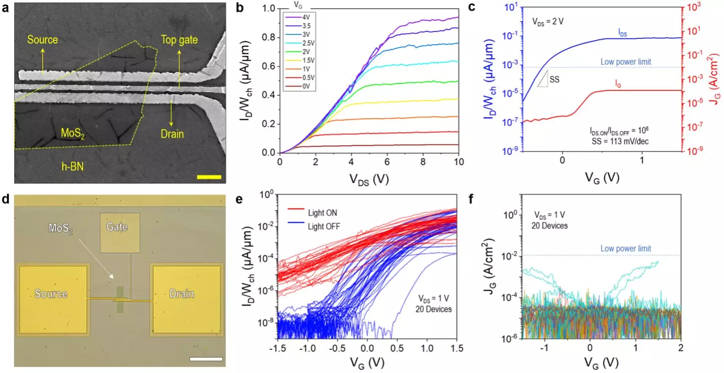
The groundbreaking approach introduced by the research team involves utilizing hexagonal boron nitride (h-BN) dielectrics in combination with high cohesive energy metal gate electrodes, specifically platinum (Pt). By employing Pt as the anode, the team discovered that the h-BN stack exhibited reduced dielectric breakdown, resulting in enhanced transistor performance. Through extensive experimentation, it was revealed that Pt/h-BN gate stacks showed a 500-times lower leakage current compared to Au/h-BN gate stacks, demonstrating a high dielectric strength of at least 25 MV/cm. This innovative design prompted the researchers to explore the potential of using chemical vapor deposited h-BN as a gate dielectric in 2D transistors.
To validate their hypothesis, Shen, Prof. Mario Lanza, and their collaborators fabricated over 1,000 devices incorporating chemical vapor deposited h-BN as dielectrics. The fabrication process involved intricate steps such as cleaning a SiO2/Si substrate, patterning Ti/Au electrodes using electron beam lithography, depositing MoS2 as the channel material, transferring CVD h-BN film onto the structure, and finally patterning the Pt gate electrode using e-beam lithography. The clean van der Waals interface between MoS2 and h-BN in the team’s transistor design significantly enhanced reliability and performance, showcasing the effectiveness of high cohesive energy metals like Pt and tungsten (W) in conjunction with CVD h-BN as an efficient gate dielectric for 2D transistors.
The outcomes of the research efforts demonstrated a significant reduction in leakage currents and a remarkable dielectric strength of at least 25 MV cm-1, positioning 2D semiconductor-based transistors as a promising avenue for the development of solid-state microelectronic circuits and devices. The use of Pt and W-based gate electrodes in conjunction with h-BN dielectrics showcased a substantial improvement in transistor performance compared to conventional Au electrodes. The findings from this study may inspire other research groups to explore similar materials and techniques, potentially paving the way for the creation of high-performance 2D semiconductor-based devices. As the researchers look towards the future, their next objective involves the development of ultra-small, fully 2D transistors to support the advancement of Moore’s Law.
Leave a Reply
You must be logged in to post a comment.